


The 1/2013 issue of LFI (Leica Fotografie International) offers insights by the creators of the Leica M’s Max sensor and Maestro processor. The leading brains in the matter share their knowledge on how it all came about. Here are some excerpts from LFI 1/2013. For the full article order the magazine’s print issue.
Leica developed the new sensor, the Max, together with the Belgian company CMOSIS. The M’s processor, the Maestro, is jointly produced with Fujitsu Semiconductor.
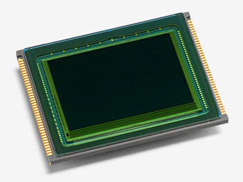
Well Leica obviously didn’t completely miss the digital photography boat. The CMOS sensor turns the M Typ 240 into a little sensation. Leica didn’t just combine prefabricated parts to assemble a camera. Rather, the German boutique camera maker was committed to develop the components itself.
The magazine spoke with Dr. Volker Zimmer, head of the digital imaging department at Leica, with Guy Meynants, founder and chief technical officer of CMOSIS, and with Mike Fraizer, key account manager at Fujitsu Semiconductor.
Asked how the collaboration between CMOSIS and Leica came about, Volker Zimmer says:
It wasn’t easy to find a partner who could fulfill our specific requirements for the sensitivity of the sensor in relation to the incident angle because of the M’s low flange distance, considering the quality of the color filter and much more. With the M9 we were still working with microlens shifting to get a grasp on the problem, but with the M it was clear right from the beginning that the camera had to also work with the lenses of Leica’s R system, which are much more telecentric (…) The second criteria was the energy consumption, because with live view and video the sensor needs to run continuously.
Asked about the development of the Max sensor, Guy Meynants says:
For CMOSIS it began with a study of the specifications, which, may I say, were very strict and, from Leica’s side, virtually written in stone (…) We deliver the chips to Leica — based on a tailor-made design optimized for the new Leica M.
Guy Meynants goes on explaining that as a basis they used a technology developed for extremely small pixel consumer products, using a technology that is, in fact, considered for pixel gaps of 1.75 micrometers. They transferred it to 6 micrometers. Consequently, the sensor benefits from all the developments that capture light better and bring it to the pixels.
Guy Meynants:
This brought us major advances in performance. Though it may seem obvious, considerable know-how is required to be able to transfer a design to a large surface, to adapt the analog-digital converter, and to keep noise low.
So AD converters are no longer on an external chip like they used to be?
Volker Zimmer:
No, they are integrated in the sensor chip. If you take a close look at the Max sensor, you can recognize below the light-sensitive area an AD converter for every one of the 6,000 columns it contains.
Guy Meynants explains that with CMOS sensors it is quite possible to integrate further switches such as the AD converter here. They use a patented two-step process called “digital correlated double sampling” which reduces noise very effectively. For this sensor CMOSIS uses the technology in combination with an AD conversion with 14-bit precision and for the performance required for 1080p video. The converter has to be extremely fast for these tasks.
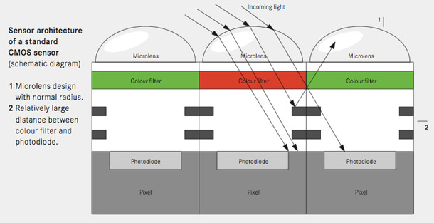
Regarding incident angle, as a basis they used a technology for very small pixels in consumer equipment. There is a lack of space there too, so the high incident angle of the light in the corners is a big issue.
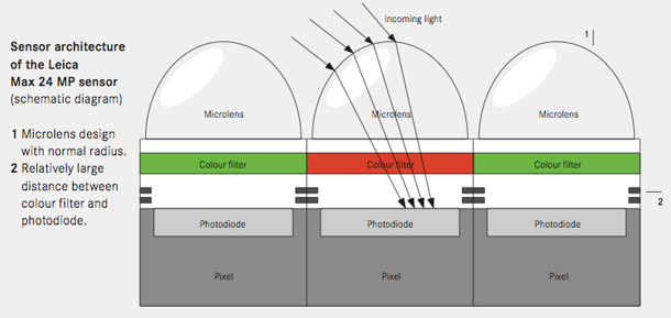
Despite the larger pixels they were able to retain the composition of the layers and their thickness.
In the case of the Max sensor, the conducting paths are not made out of the usual aluminum, but out of copper. This makes them particularly thin, so that the filter and the specially shaped microlens shift closer to the chip, making it more sensitive to the light’s incident angle.
Guy Meynants:
We only used two metal layers for the conductor, where four are normally necessary. Thanks to an advanced manufacturing process, the conductors lie around the pixels in little depressions, so that the filters move over even closer to the pixels. In addition, we don’t use the normal aluminum for the conducting paths, but rather copper. Copper is only rarely used, and then for exceptionally high-end sensors, because the manufacturing process is much more complex. Copper, however, has the advantage of having considerably lower resistance, which is why the conductors turn out only half as thick.
What role does energy consumption play? The sensor is constantly running in live view mode, that can heat sensors in such a way that increased noise appears.
Guy Meynants:
We only read each pixel with 14-bit precision in stills mode; in video mode we concentrate pixels before digitalization and, consequently, save energy in the converters. And we have very efficient AD converters.
Asked if the M’s CMOS sensor behaves like most others by processing the picture significantly before saving it, Volker Zimmer explains this happens to some degree. For example, to reduce the static noise that the specific sensor in the camera causes:
That’s totally normal, but our philosophy is not to manipulate the data while it’s still in the camera, but to transfer it as directly as possible into the computer. That’s also why we use DNG format, which allows the photographer to freely choose his or her software, and where we can hide nothing which could be possible with a proprietary format and our own software.
So how fast is the Max sensor in fact? The Maestro processor is identical to the one in the S, but it is activated by a completely different firmware and uses functions that were still more or less dormant in the S2.
Leica sticks to this chip which isn’t latest generation engineering, but makes sense for cost reasons. As a consequence, in film mode at HD setting, the M is limited to 25 images per second.
Leica won’t confirm a Maestro 2 in the making, Volker Zimmer says Leica has been working on that for a long time, but they won’t stop after the Maestro 2 either.
Speed is unfortunately one of the limits of the processor, concedes Mike Fraizer:
The sensor could deliver more than the Maestro processor is able to deal with at this time.
In closing the article, the interviewer raises the specter of small format cameras with close to 40MP output. Wouldn’t that have worked for the Leica M?
Guy Meynants says production costs for large sensors remain high. Every manufacturer has the same problem with yield. On every silicon wafer there are a certain number of unavoidable defects, and the more chips you can cut out of it, the better the chance that a certain number of functioning sensors remain.
Leica, says Volker Zimmer, must always keep an eye on the costs, and in addition to the optics, the quality of the individual pixels determines the picture results:
It’s not just about lots of pixels — they have to be good pixels; so it’s a question of finding the right balance.
The M’s strict requirement was for maximum picture quality, so they were more conservative with the pixel size. With the M, it is suggested, Leica achieved optimal picture quality.
+++ BTW, the Leica M can be ordered from Amazon (black/silver), B&H (black/silver) or Adorama (black/silver).